Memory components (RAM and ROM)
ROM
For the definition of the ROM acronym please see
http://en.wikipedia.org/wiki/Read-only_memory.
In the Logic Circuit program ROM has one input pin allowing setting the address of the data,
and one output pin set to the value of the memory cell located at the provided address.
There is no extra signals should be set in order to read the data and of course there no way to change the data in the ROM via its pins.
However the ROM can be "programmed" or filled with desired values in the edit mode of the Logic Circuit program.
In order to do these double click the ROM’s symbol on your circuit and the ROM dialog will pop up.
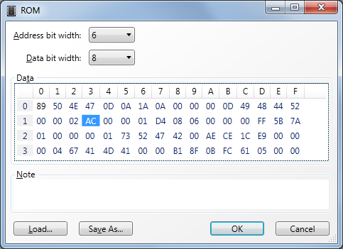
In the dialog you can change bit width of both address and data pins.
When you changing bit width of the address pin you will see the number of
available cells get updated while changing of the data bit width will affect the size of each cell.
The number of cells is a power of 2 of the address bit width and the maximum number allowed in each cell is power of 2 of data bit width.
In order to change value stored in a cell click it in the Data greed or move focus in
the greed and navigate to the desired cell with you arrow keys and just type a new value.
Value must be entered in hexadecimal format.
You can also load values from a binary file. In order to load content of file in the ROM click "Load..." button. To save it in a file click "Save..." button.
RAM
For the definition of RAM acronym please see http://en.wikipedia.org/wiki/RAM.
In the Logic Circuit program RAM has 3 input pins and one output.
The first input pin is address pin where you can select the cell you are reading or storing the data to.
The second pin is input data pin. The circuit should send the data to store to this pin.
The third input pin is one bit RAM write signal. The data get stored when the value on this pin is changing in the specified way.
In order to specify the time of storing the data double click symbol of the RAM on your circuit and RAM dialog will pop up (see below).
The only output pin of the RAM is output data. It works exactly like output pin of ROM.
When circuit gets powered up the RAM gets initialized.
By default it initialized to random values, but you can choose to set all its bits to zeros, ones or preserve values between circuit runs.
In the last case you can also edit values in the memory in the edit mode in the RAM dialog.
In order to change RAM’s properties double click its symbol on the circuit diagram while in edit mode and RAM dialog will pop up.
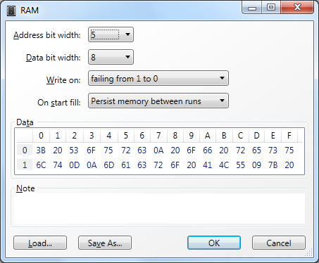
Like in ROM you can change bit width of the address and data pins.
Obviously the bit width of input data pin will be equal to bit width of output data pin so it is only one data bit width drop down there.
In the "Write on" drop down you can choose storing behavior of the RAM,
so it will store the data when signal on "RAM write" input pin will change from 1 to 0 or vice versa.
You can choose how to initialize your RAM module when the circuit is powered up.
The "Randomly" is what a real RAM module will be initialized to, so this is your primary selection. You can also set all bits to zero or one. Finally, you can save all the memory and keep it between runs. This is how a flash memory or any other storage device can work.
Please note that this option will only work if your RAM module is resided on the main circuit of your project. The reason of this restriction is if you have, such RAM in sub circuit and use it more than once than multiple values need to be stored in one RAM.
Run time
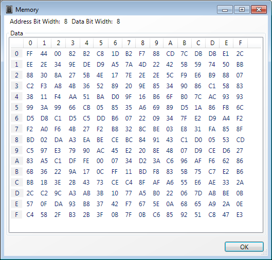
In the running mode you can browse content of the memory component by double clicking it symbol on your circuit. The memory dialog will pop up.
Please see Splitter to learn how to make multiple bits wires.
To get a feeling of the memory units please connect each of them with constants and probes and change the values and see what is the outcome is.